ZEISS Electronics & Semiconductor · Microscopy for semiconductor manufacturing
Rebuilt around how an engineer actually buys a complex instrument
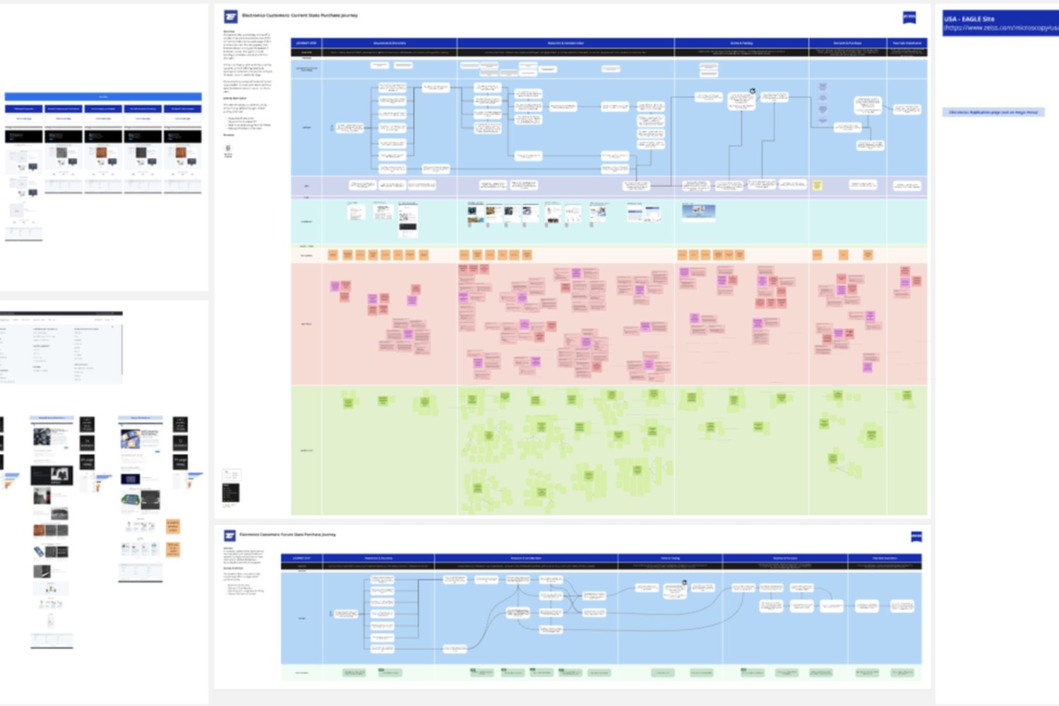
Two three-month projects — one to work out how semiconductor customers actually buy, one to build the site around the answer.
The challenge
The Electronics and Semiconductor portfolio spans wafer and die-level inspection, failure analysis, correlative light and electron microscopy, and sample preparation. Its customers are engineers and researchers working to a specific technical problem — a defect to localise, a package to inspect, a sample to prepare — not shoppers browsing a category.
The site was arranged around how ZEISS structures its own product lines, which is a rational internal logic and a poor match for how a customer arrives. Someone with a failure analysis workflow in mind has to already know which product family serves it before the navigation is any use. Add a portfolio this technically dense and the result is a customer who cannot self-serve and a sales team answering questions the site should have handled.
The second complication was that this was not a greenfield rebuild. Whatever we designed had to land inside an existing enterprise platform, alongside content production, on a timeline that gave the business something usable rather than another strategy document.
- My role
- Ran the research and built the blueprint in phase one; facilitated the new information architecture and drove the pages into staging in phase two.
- Duration
- Two three-month projects — strategy and definition, then build.
- Team
- Four of us — two leading the engagement, a designer, and an editor building the pages in AEM — working alongside the ZEISS Electronics team.
- Outcomes
A to-be journey and information architecture agreed with the business, prototypes signed off page by page, and fourteen MVP pages built and live in staging.